In production, printed circuit board (PCB), printed wiring board (PWB) and printed wiring assembly (PWA) cleaning is documented in IPC documents and manuals with relevant guidance. As technology advances, the use of more small components, high-density layouts, changes in materials, and environmental conditions have resurfaced the importance of board cleanability. The cleanability of printed circuit components has become a very challenging task.
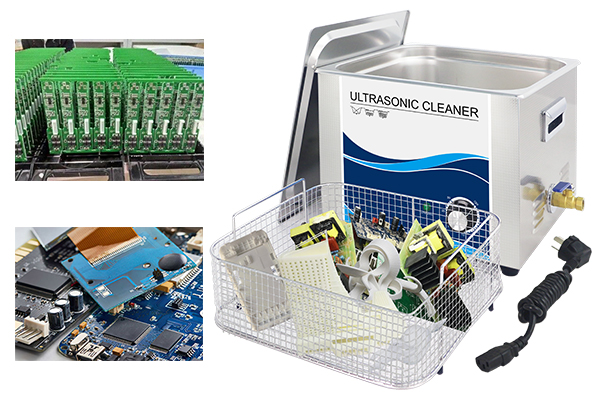
Printed circuit boards are designed, assembled and quality controlled according to established industry standards. To reduce the risk of product failure due to contamination, the cleaning process must provide a defined process window that is repeatable and covers the various variables encountered during assembly. In order to achieve a high yield cleaning process, many factors affect the cleaning process window: substrate, contaminants, available cleaning techniques, cleaning equipment and environmental factors.
(i) Substrates
The first step in designing a cleaning process is a thorough review of the printed circuit board layout to determine the plated holes, the thickness-to-diameter ratio of the holes, any through-holes suitable for plugging or masking, and the choice of soldermask material. Component composition, size and geometry can create sandwiched assemblies with low gaps and small exits, making residues difficult to remove.
Smaller, lighter parts increase the need for clamping assemblies as they pass through the cleaning process. Cleaning process design begins with consideration of board surface, metallization, and compatibility limitations. Unique limitations of components may restrict some components during the cleaning process.
(ii) Component contamination
With a clear understanding of the unique component considerations and limitations, the next step in manufacturability design is to consider the impact of contaminants left on the board after the assembly (usually soldering) process. To understand the risk of contamination, designers must consider the composition, physical properties, quantity, and ability to remove solder residue from the cleaning material. The interaction of the solder materials, i.e. the residence time between the flux and the heat treatment process associated with the component, and the residence time between the heat treatment process and the cleaning process, can have an impact on the cleanliness of the resulting component. Subsequent processing steps may also affect the cleanliness of the product. Solder paste, flux paste and wave soldering aids affect the degree and difficulty of residue removal after the soldering process. The different cleaning rates of flux residues are related to the composition of the flux, the time after reflow and the reflow temperature.
All board designs must consider the importance of these reflow factors and parameters. Solvents contain different types of intermolecular interactions: hydrogen bonds, ionic dipoles and interdipole attractions. As the amount of flux residue varies, so does the cleaning rate. For all cleaning activities, the cleaning agent and the cleaning system – including time, temperature and intensity – will affect the cleaning effect.